
DRAM
Enabling the memory yield and process control that every AI accelerator depends on
- Planar
- 4F² Vertical
- 3D DRAM
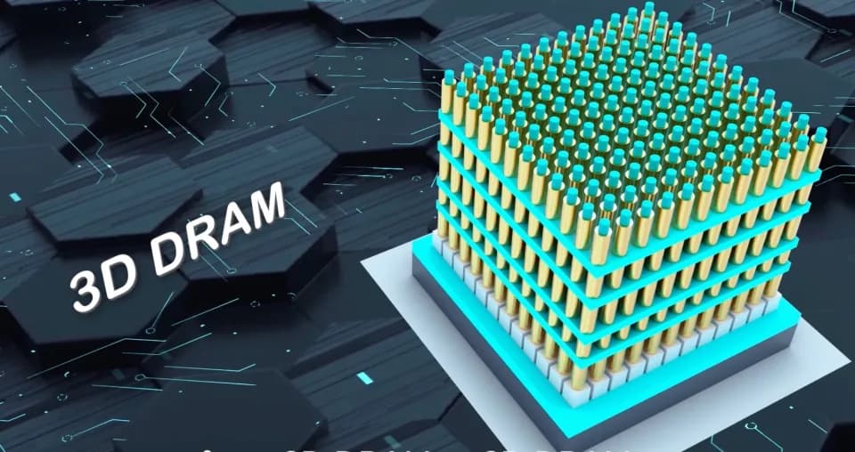
DRAM is changing architectures.
The process complexity is following.

The transition from planar DRAM cells toward vertical channel designs is a fundamental shift in DRAM architecture — and it is driving a step-change increase in the number of etch steps that require atomic-scale control.
AI accelerators are reshaping the economics of memory. Every larger model and faster training run pulls more high-bandwidth DRAM into the supply chain — and the very architectures that deliver that bandwidth are where conventional etch starts to lose its grip. Precision at the etch step is becoming a yield differentiator, not a footnote.
Where AAT Fits
For years, DRAM scaling was largely a dimensional shrink within a familiar architecture. That era is ending. As the industry moves toward vertical channel transistor architectures targeting 4F² cell geometries — and eventually to full 3D DRAM — the process flow is beginning to resemble 3D NAND in its structural complexity: high-aspect-ratio stacks, buried bitline formation, and capacitor trench profiles that demand etch precision far beyond what RIE can reliably deliver.
AAT's platform addresses the precision finishing steps in DRAM fabrication — gate recess uniformity, capacitor trench profile finishing, and the emerging high-aspect-ratio requirements that come with vertical channel architectures.
- 01Planar
- 024F² Vertical Channel
- 033D DRAM
Demonstrated Performance
- Synergy Factor>90%
- Linearity (R²)>0.9997
- Cycle Time~2 seconds
- Synergy Factor>80%
- Linearity (R²)>0.9947
- Cycle Time~2 seconds
Source: SPIE Advanced Lithography + Patterning 2026, Paper 13984-24
The AAT Advantage
Precision at production throughput.
The architecture transition in DRAM means more ALE steps per wafer — but those steps still need to hit aggressive cycle time targets. At ~2 seconds per cycle, AAT makes that possible without sacrificing the process control these new architectures demand.
Algorithmic process control.
AAT's platform continuously optimizes gas flow, power, and timing in real time — not as a correction mechanism, but as an active part of how the tool runs. As DRAM process flows grow more complex with each architecture generation, the ability to converge on a production-worthy recipe quickly becomes a meaningful competitive advantage.
The same tool, both modes.
The transition from bulk capacitor recess to precision surface finishing — two process modes that would traditionally require separate tooling — is handled within the same chamber, switched algorithmically. No manual recipe intervention required, as your process flow evolves.