// Company

The only atomic layer etch platform
designed AI-native from the ground up.

Applied Angstrom Technology is a deep-tech semiconductor equipment company, built from scratch for atomic-level precision in the Angstrom Era.

// About us

Who We Are

Applied Angstrom Technology (AAT) is a deep-tech semiconductor equipment company that has built the first atomic layer etch platform designed AI-native from the ground up.

We were founded on a straightforward conviction: the semiconductor industry's transition to sub-3nm logic nodes, 3D memory architectures, and silicon photonics requires a fundamentally different hardware and software architecture to etch precision — one that conventional tools were never built to deliver.

AAT was engineered from a clean sheet to deliver atomic-scale precision in the angstrom era. Every architectural decision — from the decoupled chamber design to the AI process control layer — was made with one uncompromising mandate: atomic-scale precision and production-worthy throughput, built in from the first line on the drawing board.

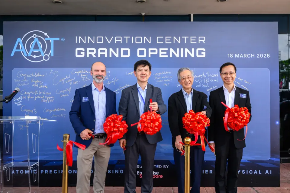
AAT leadership at the Innovation Center grand opening, 18 March 2026
Grand Opening of AAT’s Atomic Precision Innovation Center
// What drives us

Mission, vision & values

VisionMissionValues
What we're building

Vision

To develop and deliver atomic-level precision process equipment for the world's most advanced semiconductor manufacturing.

// Milestones

Our trajectory through the Angstrom Era

AchievedPlanned
2023

Foundation

  • Company founded
  • Core team assembled
2024

MVP

  • MVP tool design complete
  • MVP assembly completed
  • Initial patents filed
2025

Alpha

  • Process recipe validation
  • Partnership with Sioux Technologies
  • Internal testing on Alpha tool
  • SPIE Paper — peer-reviewed results
Now
2026+

Scale-Up

  • Atomic Precision Innovation Center
  • Demo tools ready
  • Development system shipments
  • Production qualification
  • Manufacturing Ramp
  • Worldwide expansion
// Global presence

Global Presence

AAT is headquartered in Singapore at the One-North innovation district, home to our R&D center, cleanroom facility, and core engineering team. Our presence extends to the United States, where we support business development and strategic partnerships with the world's leading semiconductor manufacturers.

World map marking Applied Angstrom Technology's locations: headquarters in Singapore and business development in the United StatesSingaporeUnited States
// Leadership

Leadership

Semiconductor industry veterans across the industry:

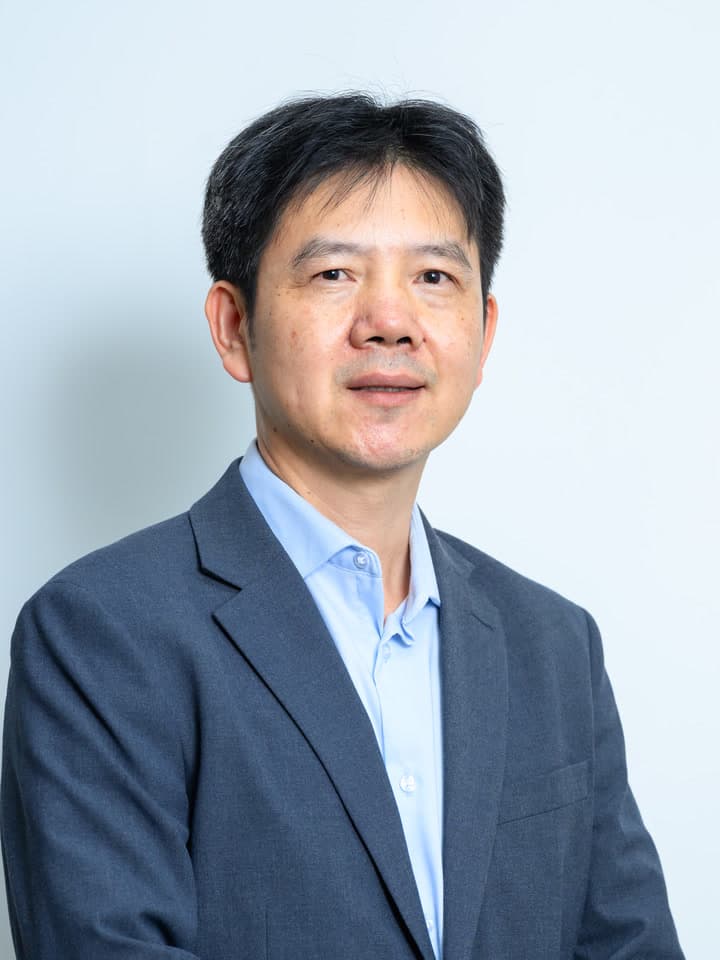
Richard Yang, Ph.D., Founder & CEO

Richard Yang, Ph.D.

Founder & CEO

10 years at Applied Materials and Lam Research in ALE and etch process and equipment development, plasma source engineering, and gas delivery systems. Led Intel 3D NAND process architecture and equipment selection. Deep expertise in leading-edge etch technology, chamber design, and AI-driven process control.

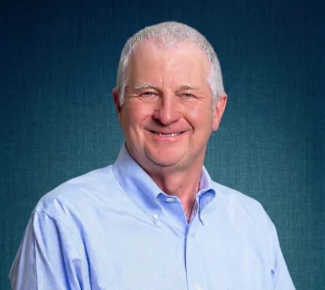
Curt Vass, Executive Advisor

Curt Vass

Executive Advisor

30+ years building and scaling semiconductor equipment businesses across logic, DRAM, and 3D NAND. Leadership roles across Applied Materials, KLA, Lam Research, and Ichor. Launched multiple products into high-volume manufacturing. MS, Stanford University.

Eddy Khoo, Operations Director

Eddy Khoo

Operations Director

20+ years of industrial operations leadership across Applied Materials, GlobalFoundries, STATS ChipPAC, AMS Osram, Nanofilm, and Celestica.

Desmond Lin, Engineering Director

Desmond Lin

Engineering Director

Principal Engineer at MIT, LightHaus Photonics. 25+ years' experience in semiconductor equipment design.

// Investors

Backed by

iGlobe Partners
SEEDS Capital
// Advisors

Advisors

World-class coverage across all aspects of the semiconductor industry, device design, process and equipment development, fundamental research and materials science.

  • Ted Taylor, Logic & Memory Expert

    Ted Taylor

    Logic & Memory Expert

    25+ years in the semiconductor industry. VP-level roles at Intel, a decade at Micron, and involvement in ASML's EUV lithography development team. Deep expertise in transitioning advanced process tools from development to high-volume manufacturing.

  • Brandon Wang, EDA Strategy Expert

    Brandon Wang

    EDA Strategy Expert

    VP Corporate Strategy at Synopsys. 20+ years across Cadence, Arm, Qualcomm, and Lattice Semiconductor. MBA, Wharton School. Drives M&A strategy and ecosystem partnerships across the semiconductor design and manufacturing stack.

  • Wes Graff, Materials Expert

    Wes Graff

    Materials Expert

    30+ years spanning process engineering and BD with deep expertise in ALD/ALE, etch/clean technologies, and Asia operations.

  • Professor Erwin Kessels, ALD / ALE Research

    Professor Erwin Kessels

    ALD / ALE Research

    Ph.D. Applied Physics, Eindhoven University of Technology. 20+ years of ALD and ALE research. Founder of the ALD Academy. Recipient of the AVS Peter Mark Award and the ALD Innovation Award (2019). Acknowledged in AAT's SPIE 2026 paper for contributions to ALE process design and validation.

  • Professor Hang Chang Chieh, Strategic Business & IP Expert

    Professor Hang Chang Chieh

    Strategic Business & IP Expert

    Ph.D., University of Warwick. Emeritus Deputy President, National University of Singapore. Founding Chairman, Intellectual Property Office of Singapore (IPOS). 50+ years of research. Recipient of the National Science & Technology Medal (2000).

// Get in touch

Deep expertise. Startup speed. Real results

Talk to our team about process development, equipment demonstration, or partnership opportunities.